题 目: 基于DSP的三相变频变幅逆变电源设计
摘要:随着社会的需求越来越高,传统的模拟电源的诸多缺陷越来越凸显, 本文在借鉴国内外相关研究的基础上,通过对空间矢量脉宽调制算法的分析,研究了数字信号处理器生成SVPWM 波形的实现方法及软件算法。并将相关方法应用于实践,研制了基于TMS320F2812数字控制的三相逆变电源,相关试验参数和结果表明:该设计提高了直流电压的利用率,使开关器件的损耗更小。此外,还提出了逆变电源闭环控制的PI控制算法,利用DSP的强大的数字信号处理能力,提高了系统的响应速度。经测试,系统实现了1~40V步进为1V的调压输出, 50Hz~1kHz步进2Hz的调频输出,输出电压恒定为36V时负载调整率小于5%。
关键词:全桥逆变,SVPWM,DSP
Abstract: With the growing demand of the society, many deficiencies of the traditional analog power become more and more obvious. Based on the related internal and international study and the analysis of space vector pulse width modulation algorithm, a kind of SVPWM waveform implementation and its software algorithms generated by digital signal processor are studied in this paper. With the methods used in practice, a digital control three-phase inverter power based on TMS320F2812 is developed. Relevant test parameters and results show that the design has improved the utilization of the DC voltage, thus making the loss of the switching device smaller. In addition, the closed-loop PI control algorithm is introduced in the inverter power. By the use of the powerful DSP digital signal processing capabilities, the response speed of the system is greatly improved. The system has been tested to achieve 1 ~ 40V voltage output regulated with 1V step, and 50Hz ~ 1kHz frequency output modulated with 2Hz step. When the output voltage keeps constant at 36V, its load regulation is less than 5%.
Key words: full bridge inverter SVPWM DSP
目录
题 目: 基于DSP的三相变频变幅逆变电源设计
1. 引言
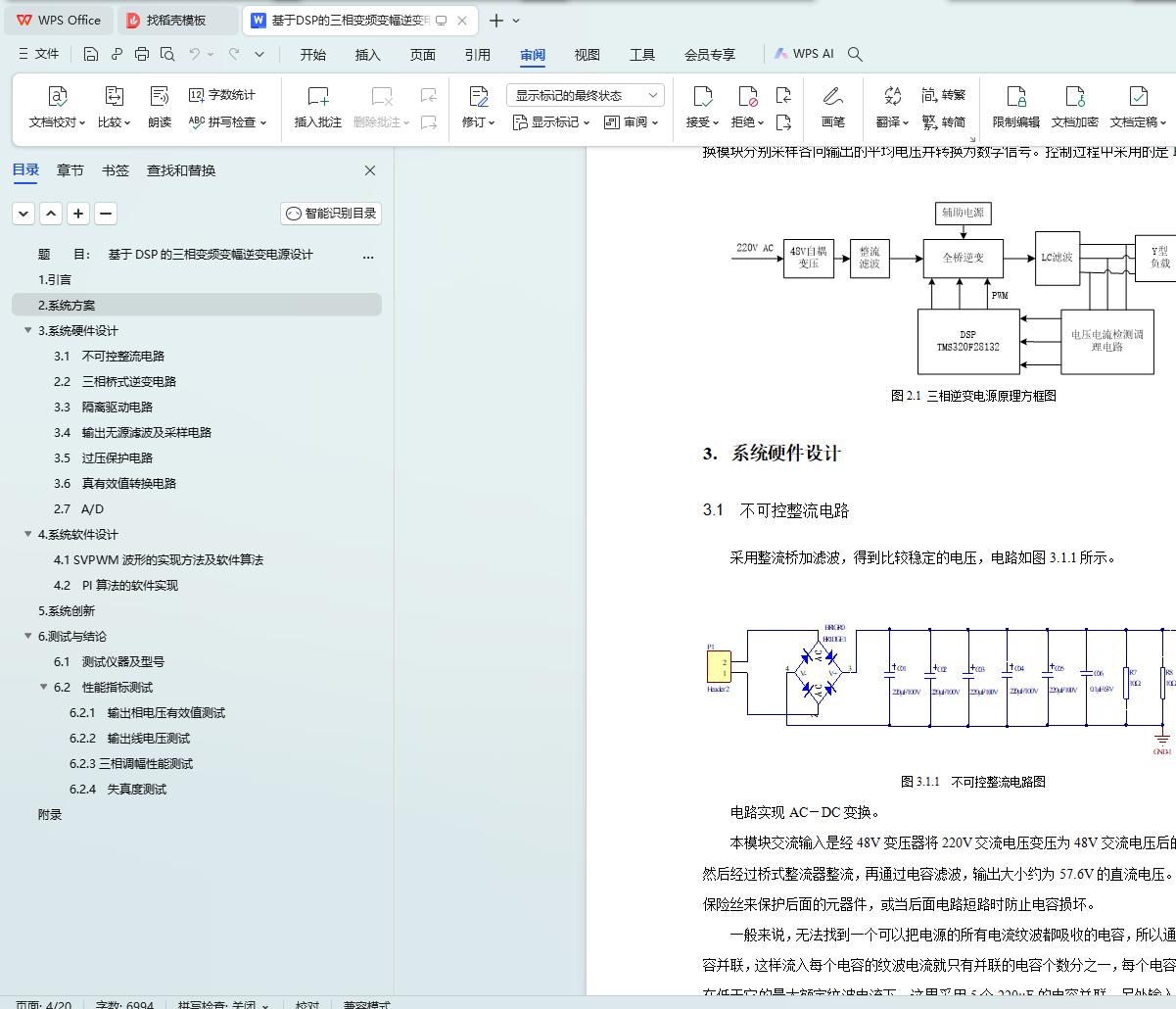
2. 系统方案
3. 系统硬件设计
3.1 不可控整流电路
2.2 三相桥式逆变电路
3.3 隔离驱动电路
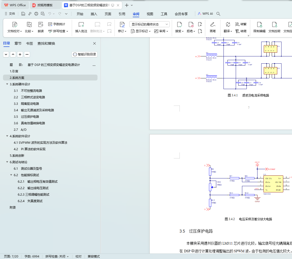
3.4 输出无源滤波及采样电路
3.5 过压保护电路
3.6 真有效值转换电路
2.7 A/D
4. 系统软件设计
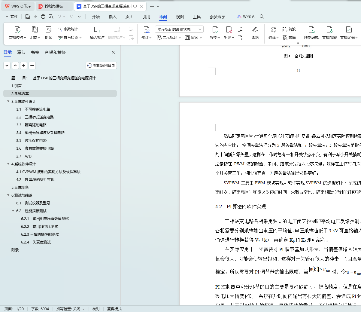
4.1 SVPWM波形的实现方法及软件算法
4.2 PI算法的软件实现
5. 系统创新
6. 测试与结论
6.1 测试仪器及型号
6.2 性能指标测试
6.2.1 输出相电压有效值测试
6.2.2 输出线电压测试
6.2.3三相调幅性能测试
6.2.4 失真度测试
附录
