摘要
随着微处理器与数字处理器的发展,需要为它们提供更低的输出电压,更大的电流。因此,对低压大电流正激变换器及其相关技术的研究,在近几年得到广泛的关注。
本文首先介绍了传统正激变换器高频变压器磁复位技术,比较了各种磁复位拓扑的优缺点,最后选择了有源箝位正激变换器作为本次设计的主拓扑。其次,分析了有源箝位正激变换器的工作过程,并对其中的典型参数进行了计算推导。再次,在分析了三种驱动方式的基础上,对有源箝位正激变换器专用驱动芯片NCP1562进行管脚功能介绍,以及外围电路的搭建。主要包括辅助电源,过流、过欠压保护,振荡频率,误差反馈输入等相关电路的设计。最后,完成器件的参数计算,器件的最终选型,并采用MATLAB对系统进行仿真。得到电压、电流的输出波形,完成了对波形的简要分析,论证了理论分析的正确性和设计方案的可行性。
关键词 正激变换器 有源箝位 变压器磁复位
Abstract
With the development of microprocessor and digital processor, lower output voltage and higher current is needed to provide. Therefore, research on lower output voltage and higher current forward converter is widely focused on.
Firstly, the high frequency transformer magnetic reset technique of traditional forward converter is introduced in this paper. The advantage and disadvantage of various magnetic reset topologies is compared. An active clamp forward converter is chosen as the main topology of this design. The working process of active clamp forward converter and the typical parameters of the calculation and derivation are analyzed. Thirdly, based on analysis of the three driving modes, pin function of the active clamp forward converter drive chip NCP1562 is introduced and the peripheral circuit is constructed. Mainly includes the auxiliary power supply, over-current protection, over-voltage or under voltage protection, oscillation frequency, error feedback input and so on. Finally, the calculation of parameters of the device, the final selection device, and use MATLAB to simulate system is completed. The output waveform of voltage and current is briefly analyzed. The correctness and feasibility of the theoretical analysis of the design scheme is proved.
Keywords Forward converter Active clamp Transformer magnetic reset
目 录
摘要
Abstract
第1章 绪论
1.1 课题背景
1.1.1 开关电源的发展
1.1.2 选题目的及意义
1.2 开关电源
1.2.1 开关电源定义
1.2.2 开关电源基本结构
1.2.3 开关电源特点
1.3 研究的主要内容
第2章 正激变换器
2.1 传统单端正激变换器
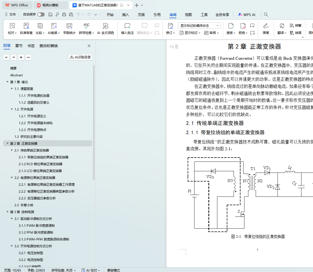
2.1.1 带复位绕组的单端正激变换器
2.1.2 RCD箝位单端正激变换器
2.1.3 LCD箝位单端正激变换器
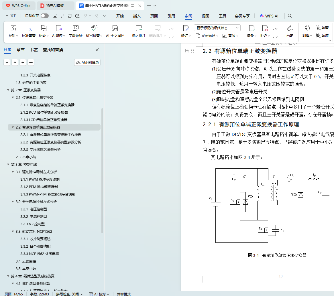
2.2 有源箝位单端正激变换器
2.2.1 有源箝位单端正激变换器工作原理
2.2.2 有源箝位正激变换器典型参数分析
2.2.3 变压器磁芯参数分析
2.3 本章小结
第3章 控制电路
3.1 驱动脉冲调制方式分析
3.1.1 PWM脉冲宽度调制
3.1.2 PFM脉冲频率调制
3.1.3 PWM-PFM脉宽脉频综合调制
3.2 开关电源控制方式分析
3.2.1 电压控制型
3.2.2 电流控制型
3.2.3 V2控制型
3.3 驱动芯片NCP1562
3.3.1 芯片简要概述
3.3.2 各个引脚功能
3.3.3 NCP1562外围电路
3.4 反馈回路
3.5 本章小结
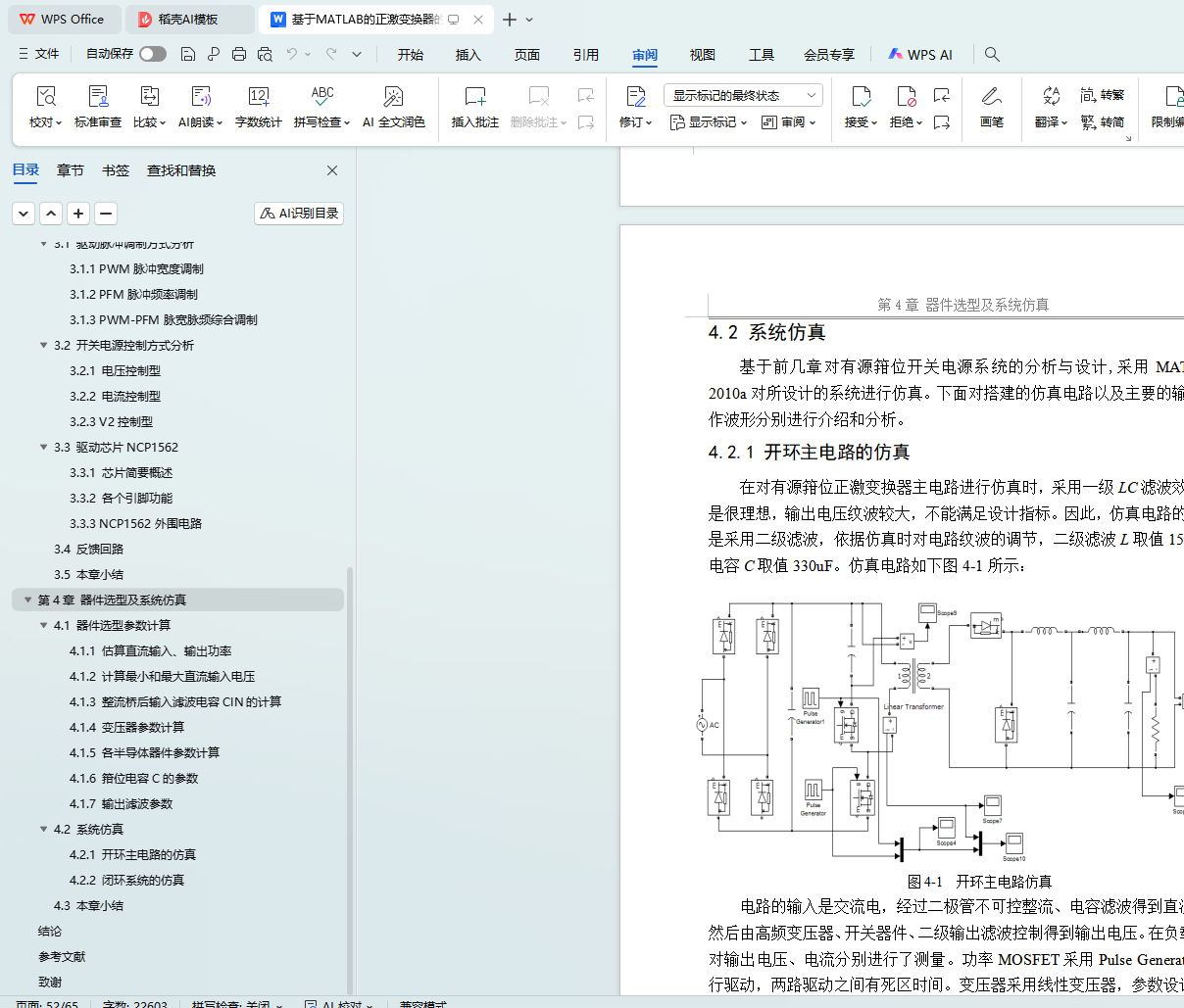
第4章 器件选型及系统仿真
4.1 器件选型参数计算
4.1.1 估算直流输入、输出功率
4.1.2 计算最小和最大直流输入电压
4.1.3 整流桥后输入滤波电容CIN的计算
4.1.4 变压器参数计算
4.1.5 各半导体器件参数计算
4.1.6 箝位电容C的参数
4.1.7 输出滤波参数
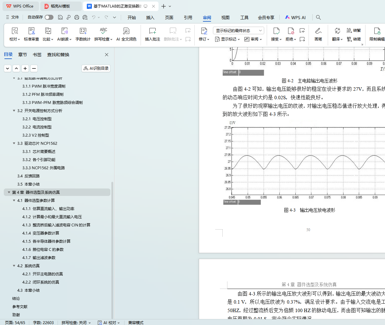
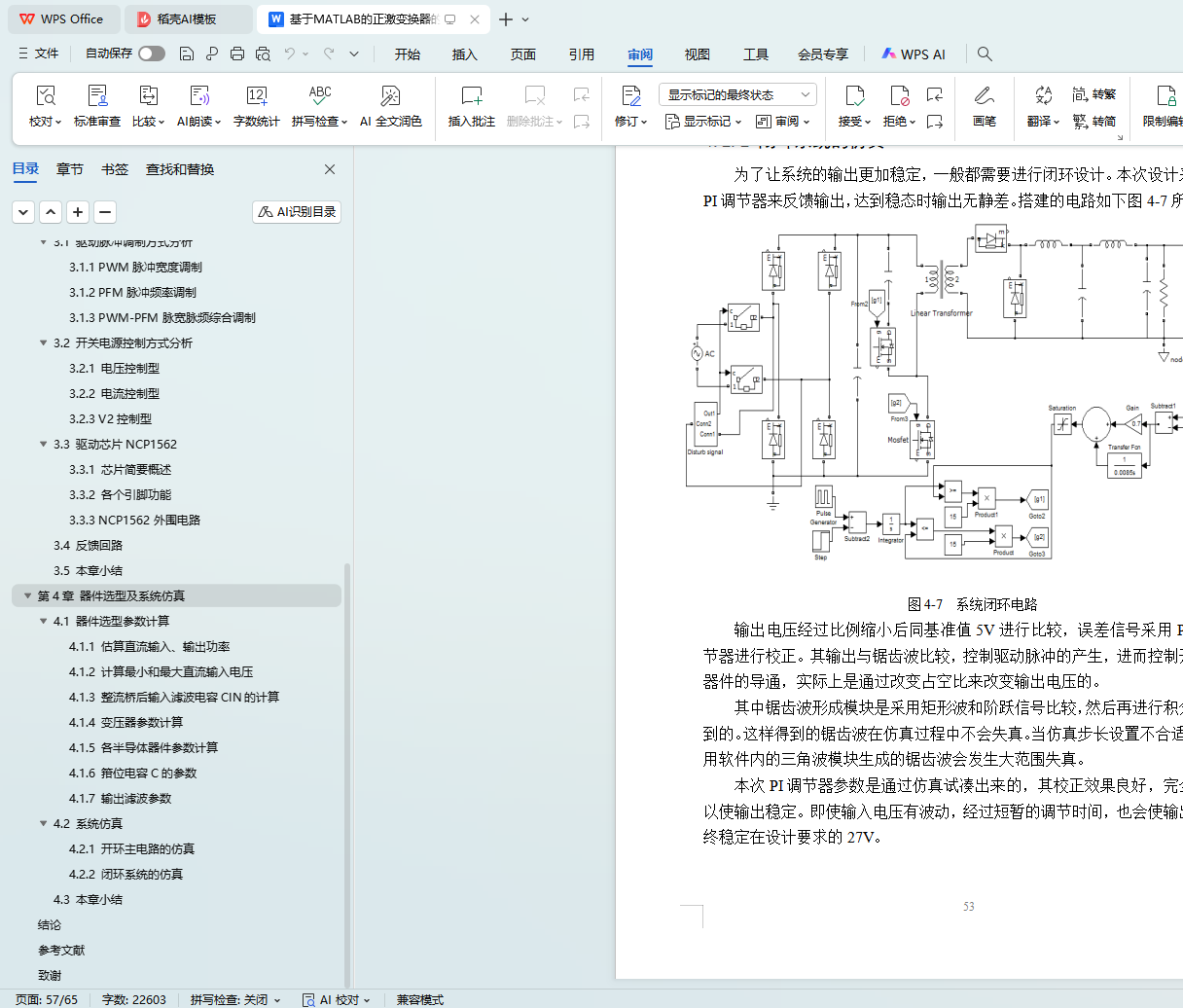
4.2 系统仿真
4.2.1 开环主电路的仿真
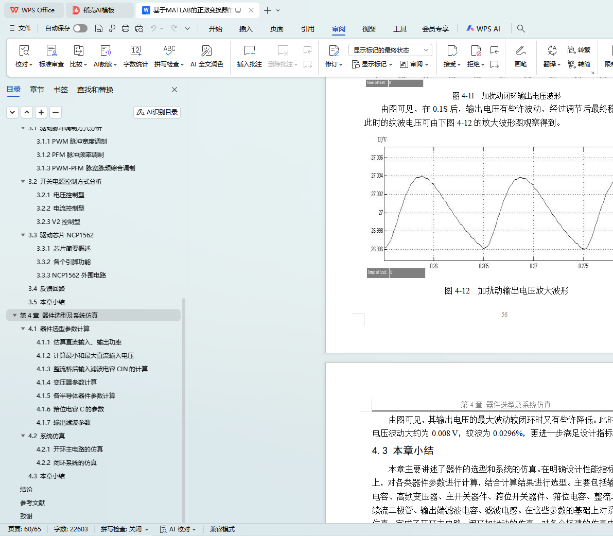
4.2.2 闭环系统的仿真
4.3 本章小结
结论
参考文献
致谢