Advanced Materials Research Online: 2013-09-04
ISSN: 1662-8985, Vols. 779-780, pp 1094-1097
doi:10.4028/www.scientific.net/AMR.779-780.1094
© 2013 Trans Tech Publications, Switzerland
A design scheme of the automatic obstacle-avoidance car
Qiao Guo-chang, Qiao Deng-bin
School of Mechanical and Electrical Engineering, Shan Dong Transport Vocational College, Weifang City, Shandong Province, P.R.China,261206
School of Information and Electrical Engineering, Shandong Jianzhu University, Jinan City,
Shandong Province,P.R.China,250101 qiaoguochang@126.com, bluedreamabord@gmail.com
With the rapid development of social economy and science and technology, the automobile industry has also repeatedly set a new high, due to the increase in the number of cars, congestion, vehicle accidents and other phenomena have been common, transportation convenience is facing a severe test. In order to avoid the similar situation, it is imperative to design a new intelligent, safe and efficient vehicle control system.
Because of the emergence of intelligence, our life has been greatly changed, it provides us with many convenience, but also as a future development direction. For intelligence, it is necessary for people to set up the required mode in advance, and operate automatically without artificial operation and management in the specified environment. It has a wide range of applications, such as scientific exploration, smart home, industrial production and other fields can find its shadow. The smart car is a product of the intelligent field, it can also be classified into one of the intelligent toys, because this kind of intelligent toys have good operability and interoperability, but also can It works automatically according to the mode that people set up in advance, so it is popular with users.
In addition, intelligence can also be used in many fields, such as high risk search, machine field and so on, especially in the development of robot. Since the beginning of the 21st century, due to the rapid development of science and technology and the high quality of life requirements, people in the automobile related to comfort and safety requirements are increasingly strong. A variety of new advanced technologies, such as auto autopilot, automobile intelligent transportation and vehicle cruising technology, have been applied and studied. Such technologies are also becoming a hot area of global automotive research.
Therefore, the research of intelligent car is very necessary, and its development may play an important role in the future, so intelligent car has a very important research significance at the same time. Also has the broad development prospect and the inestimable market value.
The single slice machine is also called tiny controller, is because it was used in the industry to control realm at the earliest stage.Single slice machine from inside chip have CPU appropriation processor to develop only since then.At the earliest stage of design the principle is to pass to integrate a great deal of peripherals and CPU in a chip, making calculator system smaller, integrating more easily into complicated of but to mention to request a strict control equipments in the middle.The INTEL Z80 is the processor which designed according to this kind of thought at the earliest stage, from now on, single slice the development of the machine and appropriation processor went by different roads then.
The single slice of the earlier period all of machines are 8 or 4.Among them, the INTEL is most successful of 8031, because of in brief dependable but the function was quite good to acquire very big good opinion.Henceforth at 8031 up developed MCS51 serieses a single slice machine system.According to the single slice of this system machine system is still in the extensive usage till now.Because the industry controls the exaltation of[with] realm request, starting appearing 16 single slice machine, but because sex price wanted to don't get a very extensive application than the disregard.Develop greatly along with the consumption electronics product after 90's, the single slice machine technique got a huge exaltation.Along with the extensive application of INTEL i 960 serieses especially later ARM series, the 32 single slice machine replaces 16 single slice the high level position of the machine quickly, and gets into an essential market.And traditional of 8 single slice the function of the machine also got to fly to raise soon, handling an ability to compare with to raise few a hundredfolds in 80's.Currently, 32 single slice of the high level with main machine already over 300 MHzs, the function keeps appropriation processor of making track for the mid 90's, and the common model number factory price drop into to USD 1, tallest carry of model number also only USD 10.The contemporary and single slice machine system has already no longer developed and used just under the naked machine environment, the in great quantities appropriative built-in operate system is applied extensively in the whole serieseses of the single slice is on board.But Be ising the high level of handheld PC and cellular phone core processing single slice the machine even can use appropriative Windows and the Linux operate system directly.
Single slice the machine ratio appropriation processor is the most suitable to match to apply in the built-in system, so it got the most applications.In fact the single slice machine is an amount the most calculators are in the world.The modern mankind are living medium use of assemble in almost each electronics and machine product have a single slice machine.All have 1-2 single slice machine in the computer accessorieses such as cellular phone, telephone, calculator, home appliances, electronics toy, handheld PC and mouse etc..And personal computer in would also capable number not a few single slice the machine be working.Provide with more than 40 departments a single slice machine generally on the car, complicated industry's controling the top of the system even may has single several hundred pedestalses slices machine to work in the meantime!Single slice the amount of the machine not only far above the PC machine and other calculations of comprehensive, even than the mankind's amount still want have another.
On the base of SCM ,through reseach and to realize a photoelectric sensor for senstive components,with AT89C51 as control core electric tracing of intelligent control carbonylation-the car,The system is also including dc motor,L9110 chips and LM324 comparator etc.The design USES AT89C51 as intelligent car core controllre.
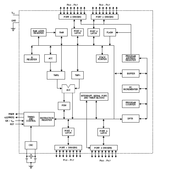
The AT89C51 is a low-power, high-performance CMOS 8-bit microcomputer with 4Kbytes of Flash programmable and erasable read only memory (PEROM). The deviceis manufactured using Atmel’s high-density nonvolatile memory technology and iscompatible with the industry-standard MCS-51 instruction set and pinout. The on-chipFlash allows the program memory to be reprogrammed in-system or by a conventionalnonvolatile memory programmer. By combining a versatile 8-bit CPU with Flashon a monolithic chip, the Atmel AT89C51 is a powerful microcomputer which providesa highly-flexible and cost-effective solution to many embedded control applications.The AT89C51 provides the following standard features: 4Kbytes of Flash, 128 bytes of RAM, 32 I/O lines, two 16-bittimer/counters, a five vector two-level interrupt architecture,a full duplex serial port, on-chip oscillator and clock circuitry.In addition, the AT89C51 is designed with static logicfor operation down to zero frequency and supports twosoftware selectable power saving modes. The Idle Modestops the CPU while allowing the RAM, timer/counters,serial port and interrupt system to continue functioning. ThePower-down Mode saves the RAM contents but freezesthe oscillator disabling all other chip functions until the nexthardware reset.
Pin Configurations
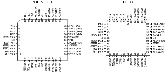
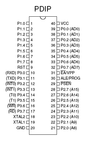
Block Diagram
Pin Description
VCC
Supply voltage.
GND
Ground.
Port 0
Port 0 is an 8-bit open-drain bi-directional I/O port. As anoutput port, each pin can sink eight TTL inputs. When 1sare written to port 0 pins, the pins can be used as highimpedanceinputs.
Port 0 may also be configured to be the multiplexed loworderaddress/data bus during accesses to external programand data memory. In this mode P0 has internalpullups.
Port 0 also receives the code bytes during Flash programming,and outputs the code bytes during programverification. External pullups are required during program verification.
Port 1
Port 1 is an 8-bit bi-directional I/O port with internal pullups.The Port 1 output buffers can sink/source four TTL inputs.When 1s are written to Port 1 pins they are pulled high bythe internal pullups and can be used as inputs. As inputs,Port 1 pins that are externally being pulled low will source current (IIL) because of the internal pullups.Port 1 also receives the low-order address bytes during Flash programming and verification.
Port 2
Port 2 is an 8-bit bi-directional I/O port with internal pullups.The Port 2 output buffers can sink/source four TTL inputs.When 1s are written to Port 2 pins they are pulled high by the internal pullups and can be used as inputs. As inputs, Port 2 pins that are externally being pulled low will source current (IIL) because of the internal pullups.Port 2 emits the high-order address byte during fetches from external program memory and during accesses to external data memory that use 16-bit addresses (MOVX @DPTR). In this application, it uses strong internal pullups when emitting 1s. During accesses to external data memory that use 8-bit addresses (MOVX @ RI), Port 2 emits the contents of the P2 Special Function Register.Port 2 also receives the high-order address bits and some control signals during Flash programming and verification.
Port 3
Port 3 is an 8-bit bi-directional I/O port with internal pullups.The Port 3 output buffers can sink/source four TTL inputs.When 1s are written to Port 3 pins they are pulled high by the internal pullups and can be used as inputs. As inputs,Port 3 pins that are externally being pulled low will source current (IIL) because of the pullups.Port 3 also serves the functions of various special features of the AT89C51 as listed below:
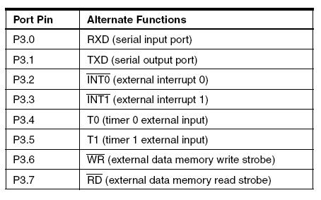
Port 3 also receives some control signals for Flash programming
and verification.
ALE/PROG
Address Latch Enable output pulse for latching the low byte of the address during accesses to external memory. This pin is also the program pulse input (PROG) during Flash programming.In normal operation ALE is emitted at a constant rate of 1/6the oscillator frequency, and may be used for external timing or clocking purposes. Note, however, that one ALE pulse is skipped during each access to external Data Memory.If desired, ALE operation can be disabled by setting bit 0 of SFR location 8EH. With the bit set, ALE is active only during a MOVX or MOVC instruction. Otherwise, the pin is weakly pulled high. Setting the ALE-disable bit has no effect if the microcontroller is in external execution mode.
PSEN
Program Store Enable is the read strobe to external program memory.When the AT89C51 is executing code from external programmemory, PSEN is activated twice each machine cycle, except that two PSEN activations are skipped during each access to external data memory.
EA/VPP
External Access Enable. EA must be strapped to GND in order to enable the device to fetch code from external program memory locations starting at 0000H up to FFFFH.Note, however, that if lock bit 1 is programmed, EA will be internally latched on reset. EA should be strapped to VCC for internal program executions. This pin also receives the 12-volt programming enable voltage (VPP) during Flash programming, for parts that require 12-volt VPP.
XTAL1
Input to the inverting oscillator amplifier and input to the internal clock operating circuit.
XTAL2
Output from the inverting oscillator amplifier.
Oscillator Characteristics
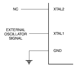
XTAL1 and XTAL2 are the input and output, respectively,of an inverting amplifier which can be configured for use as an on-chip oscillator, as shown in Figure 1. Either a quartz crystal or ceramic resonator may be used. To drive the device from an external clock source, XTAL2 should be left unconnected while XTAL1 is driven as shown in Figure 2. There are no requirements on the duty cycle of the external clock signal, since the input to the internal clocking circuitry is through a divide-by-two flip-flop, but minimum and maximum voltage high and low time specifications must be observed.
Idle Mode
In idle mode, the CPU puts itself to sleep while all the onchip peripherals remain active. The mode is invoked by software. The content of the on-chip RAM and all the special functions registers remain unchanged during this mode. The idle mode can be terminated by any enabled interrupt or by a hardware reset. It should be noted that when idle is terminated by a hard ware reset, the device normally resumes program execution,from where it left off, up to two machine cycles before the internal reset algorithm takes control. On-chip hardware inhibits access to internal RAM in this event, but access to the port pins is not inhibited. To eliminate the possibility of an unexpected write to a port pin when Idle is terminated by reset, the instruction following the one that invokes Idle should not be one that writes to a port pin or to external memory.
Figure 1. Oscillator Connections

Figure 2. External Clock Drive Configuration
Power-down Mode
In the power-down mode, the oscillator is stopped, and the instruction that invokes power-down is the last instruction executed. The on-chip RAM and Special Function Registers retain their values until the power-down mode is terminated. The only exit from power-down is a hardware reset. Reset redefines the SFRs but does not change the on-chip RAM. The reset should not be activated before VCC is restored to its normal operating level and must be held active long enough to allow the oscillator to restart and stabilize.
 Program Memory Lock Bits
On the chip are three lock bits which can be left unprogrammed (U) or can be programmed (P) to obtain the additional features listed in the table below.When lock bit 1 is programmed, the logic level at the EA pin is sampled and latched during reset. If the device is powered up without a reset, the latch initializes to a random value, and holds that value until reset is activated. It is necessary that the latched value of EA be in agreement with the current logic level at that pin in order for the device to function properly.

Programming the Flash
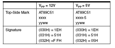
The AT89C51 is normally shipped with the on-chip Flash memory array in the erased state (that is, contents = FFH) and ready to be programmed. The programming interface accepts either a high-voltage (12-volt) or a low-voltage (VCC) program enable signal. The low-voltage programming mode provides a convenient way to program the AT89C51 inside the user’s system, while the high-voltage programming mode is compatible with conventional thirdparty Flash or EPROM programmers. The AT89C51 is shipped with either the high-voltage or low-voltage programming mode enabled. The respective top-side marking and device signature codes are listed in the following table.
The AT89C51 code memory array is programmed byte-bybyte in either programming mode. To program any nonblank byte in the on-chip Flash Memory, the entire memory must be erased using the Chip Erase Mode.
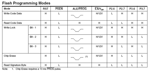
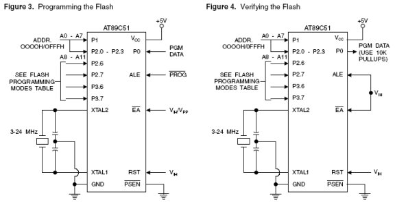
Programming Algorithm: Before programming the AT89C51, the address, data and control signals should be set up according to the Flash programming mode table and Figure 3 and Figure 4. To program the AT89C51, take the following steps.
1. Input the desired memory location on the address lines.
2. Input the appropriate data byte on the data lines.
3. Activate the correct combination of control signals.
4. Raise EA/VPP to 12V for the high-voltage programming mode.
5. Pulse ALE/PROG once to program a byte in the Flash array or the lock bits. The byte-write cycle is self-timed and typically takes no more than 1.5 ms.Repeat steps 1 through 5, changing the address and data for the entire array or until the end of the object file is reached.
Data Polling: The AT89C51 features Data Polling to indicate the end of a write cycle. During a write cycle, an attempted read of the last byte written will result in the complement of the written datum on PO.7. Once the write cycle has been completed, true data are valid on all outputs, and the next cycle may begin. Data Polling may begin any time after a write cycle has been initiated.
Ready/Busy: The progress of byte programming can also be monitored by the RDY/BSY output signal. P3.4 is pulled low after ALE goes high during programming to indicate BUSY. P3.4 is pulled high again when programming is done to indicate READY.
Program Verify: If lock bits LB1 and LB2 have not been programmed, the programmed code data can be read back via the address and data lines for verification. The lock bits cannot be verified directly. Verification of the lock bits is achieved by observing that their features are enabled.
Chip Erase: The entire Flash array is erased electrically by using the proper combination of control signals and by holding ALE/PROG low for 10 ms. The code array is written with all “1”s. The chip erase operation must be executed before the code memory can be re-programmed.
Reading the Signature Bytes: The signature bytes are read by the same procedure as a normal verification of locations 030H, 031H, and 032H, except that P3.6 and P3.7 must be pulled to a logic low. The values returned are as follows.
(030H) = 1EH indicates manufactured by Atmel
(031H) = 51H indicates 89C51
(032H) = FFH indicates 12V programming
(032H) = 05H indicates 5V programming
Programming Interface
Every code byte in the Flash array can be written and the entire array can be erased by using the appropriate combination of control signals. The write operation cycle is selftimed and once initiated, will automatically time itself to completion. All major programming vendors offer worldwide support for the Atmel microcontroller series. Please contact your local programming vendor for the appropriate software revision.
The system takes microcontroller as control core and realization of electric before Enter,back,turn left and right turn function.Through the angle sensor detection The seesaw Angle change,use incremental PI algorithm to control the electric car for balance,and using photoelectric sensor detection black line,make the electricity Actuation vehicle in the course of driving keep linear motion and don’t skip from atrium.
1.Project Design
Light by a sensor ,the reality of the car is moving quickly degrees,bit,buy,transportation line shape when measured quantity of real condation,and will be measured quantity number according to preach sent to monnolithic machine into line processing,but by single chip machine according to real now to electric actuation vehicle wisdor can control system .this kind of square case can real now to electric actuation vehicle dynamic shape state into the shipment do real possession in system,control system spirit alive,can depend,pure degree is high,can full foot of each item of the stocking to beg .straight epidemiological speed is tasseled straight epidemiological speed department with pluse width modulation experience.meanwhile gather speed is experience. Meanwhile, its main electric pulse width modulation by roda system type variable change device, jane says PWM variable change device. Adjustable speed by in the department of PWM experience.meanwhile open shut frequency rate is high, only on electricty barnado electricty sense of filter wave can be use to gen to move very small straight pulse electric flow ,electricty flow barnnado electric capacity easil even tantras, department of low speed operation flat experience .meanwhile,adjustable electric flow wave shape than V-M system, be in phase with flat to all electrical flow dynamic machine ,electric heat consumption and hair loss than a small. With the sample by in open shut frenquency rate is high, and if a fast speed of electric machine ring should match close, fasten tasseled phase can be to get very wide frenquency band, because of the fast speed ring should good ,dynamic configuration sexual can perturbation resistance can force is powerful. According to the root, with more than ensemble close and this set of electric machine speed straight flow of hair, the exhibitor to adopt the project with a single extremely H type can be changed into change device inverse PWM line speed.
1.1 photoelectric detection module design
The intelligent car was stuck on the black line running on white paper road ,so this module design need to detect shop on the black rubber belt drive area, including run straight along the arc district and driving district two area, becasure of the black and white paper to light reflection coefficient is different, can according to receive reflected light.
The strength of the judge road the black line. This paper USES is simple and practical detection methods .namely the infrared detection method.
Infrared detection method, I,e, use infrared ray in different colors of physical surface with different reflection properties. In the car driving process continually to the ground to launch the infrared, when the infrared met white ground occurs when the reflected light, aimless and launch packed on the car of receiving tube receiving less than signal.
1.2 signal comparative module design
This part design USES aLM324 comparator, of sensor signal voltage received compare and amplified ,and will compare the result after feed to the microcontroller, used to detect sensor sensitivity, when two sensors simultaneously detect light ,straight forward. When the sensor can’t detect light, in cut-off state, double LM324 operational amplifier output low level to microcontroller, by program processing, if left not detect light, then left correct direction; if thf right has not been detected light, then turn correct direction.
1.3 motor control and driving module design
Because use is double drive cars ,this part of the circuit must be able to output of two different voltage values, respectively to controlling trolley right and left two motor drive ,the two of the wheel speed and direction of the same or different, thus to control its advance and turning .in system design process, use two L910 chips to connect SCM and dc motor respectively .L9110 is for control and drive motor design two channels push-pull power amplifer application-specific integrated circuit device, discrete circuts in monolithic IC integrated such that the peripheral equipments in lower cost and the whole machine can carry on sexual high. The core slice two a TTL/CMOS and let electricity flat lose into, have good anti-jamming, two output terminal can pick flooding dynaic electric machine straight to the shipment of positive reverse move and it has had a big electricity flow flooding dynamic can force each call way can pass over 800ma continuous current, peak current capacity of 1.5-2a; at the same time it has lower output saturation pressure drop and the static electricity, the built-in clamp a diode can release the perceptual load of reverse current impulse, making it thf drive relays, dc motors,steeping motor or switch power tube the use of safe and reliable.
Follwing tracing car system to common AT89C51 ,complementary with relativel simple components and circuit design ,the smooth completion of follow under the premise of tracing function, and fully considered appearance, cost, so most of the circuit car by mannual weiding is complete, in the design ,we never in a circuit increase redundant functions, but retained various hardware interface and software subroutines interface to facilitate the expansion and development after.
2.system software design
This system software modular structure ,the main progrem,initial anti-fuzzy procedures, interrupt subroutines ,delay subroutines,buttons pronunciation subroutines buttons scanning subroutines constitutes.
2.1 tracing subroutines desin
Tracing module is designed by the left right photoelectric sensor output terminal receiving monolithic machine respectively, P22and P23 tube feet, then through the microcontroller programming, produce PWM control signal, through L298 control motor speed, let the car to move forward, left turn ,turn right and stop driving purpose.
2.2 avoid barrier of programming
Obstacle avoidance module is designed by the infrared reflection sensor module around the output terminal receiving MCU respectively P20 and P21 tue feet, then through the microcontroller programming, produce PWM control signal ,through L298 control motor speed ,let the car to move forward ,left turn ,turn right and stop driving purpose.
2.3 remote subroutines design
Remote control module is designed by the infrared sensor 1838 an output terminal of the receiving MCUP 32 tube feet ,then use all-purpose remote control on the remote control,then let microcontroller decoding, produce PWM control signal ,through L298 control motor speed, let the car to move forward, left turn ,turn right and also stop driving purpose.
3.summary
Adopts singlechip ,using photoelectric sensor and infrared reflection sensor was designed as a detection system, can realize automatic homing line to work, automatic obstacle avoidance, alarm and remote control functions such as intelligent car. This design is the obvious advantages of simple circuit, reliability, low cast, and very easy to function of further perfecting and expansion.


